微信内可能无法直接打开本站。请点右上角 ··· → 在浏览器打开,或复制链接。
How Will The Custom HBM Business Work?
RSS 官方收录 · 可信分层展示
关键摘要
Key Takeaways: HBM4 allows a customized base die, a capability that primarily targets hyperscalers.…
- Exactly how these projects proceed will vary by project, but the scarc…
- Although memory supply is tight now, cHBM isn’t expected to further bu…
- With HBM4 comes the option of customizing the base die.
摘要引擎:抽取
正文提要
Key Takeaways:
- HBM4 allows a customized base die, a capability that primarily targets hyperscalers.
- Exactly how these projects proceed will vary by project, but the scarce resource is design teams and tools.
- Although memory supply is tight now, cHBM isn’t expected to further burden demand.
With HBM4 comes the option of customizing the base die. Memory makers typically design all the layers of an HBM stack, but for a custom base die, who will design it? Who will manufacture it? And who will assemble the final stack? It turns out that the answer to those questions will vary, according to negotiations.
Custom HBM implementations (sometimes shortened to cHBM) allow companies to adapt their memory as part of an overall XPU (CPU/GPU/NPU) customization program. In a time when memory supply is stretched, adding custom memory to the already-challenged regular HBM business might seem a tough row to hoe, but custom HBM isn’t likely to further stress supply. Moreover, some recent ideas work around shortages.
Ultimately, where practical, cHBM is about differentiation. “You get into these discussions about, ‘How do I differentiate?’” said Rob Kruger, product management director at Synopsys. “One of the ways to differentiate is the cHBM model.”
A turning point with HBM4
High-bandwidth memory, or HBM, comprises many layers, each of which is a memory die except for one. The bottom die is a logic die and handles management, addressing, and other non-memory tasks that must happen within the stack. Up through HBM3, the memory makers — predominantly Micron, Samsung, and SK Hynix —fabricated all those dies in the stack, including the base die.
“In the past the base die was also the same process as a DRAM,” explained Kruger.
But that’s changed with HBM4. “For power and performance, they moved to logic processes.”
The base die needed to move to more modern finFET processes (likely 4nm or beyond), and DRAM dies aren’t doing that. So while the memory makers still design the standard base die, a logic foundry will manufacture it. The memory maker can then assemble the stack, dice the stacked wafers, and test the finished stacks.
That covers the standard base die. In addition, HBM4 and its successors let you replace the standard base die with a customized one to handle specific workloads more efficiently.
Why customize HBM?
In theory, many companies across industries could be interested in customized memory. The memory layers themselves aren’t customized, but the controlling logic can be, which is very useful for chip and system architects.
If you’re building a system with standard HBM, all you have to do is acquire the units off the shelf (at present, putting you in line with everyone else that wants some). If you decide that customizing makes sense, then instead of simply buying what you want, you now have a chip-design project to fund and manage. That immediately restricts who can do this.
In fact, this capability is largely intended for hyperscalers for three reasons. First, they have the money to do it. Second, AI processing involves a very narrow set of workload types as compared to web servers. You can even dedicate machines to one specific type of workload, which wouldn’t work as well for a web server since you may not know in advance what the workload will be.
So the hyperscalers are more likely than most to dedicate a large swath of machines to a specific workload style. Customizing the host and memory makes much more sense in that context.
The third motivator reflects the fact that while standards could be set for different workloads, the standardization process takes too long compared with the rapid pace of computing evolution for AI.
“JEDEC has been slow in standardization,” said Khurram Malik, associate vice president of data-center memory solutions at Marvell. “Hyperscalers are moving at a much faster pace, and the question becomes, ‘How to customize those HBM base dies based on their workload?’”
Customizing gives these companies a way to adapt in concert with computing advancements, rather than waiting for a formal standard. It also may give companies a differentiating edge, depending on what they customize.
Beyond hyperscalers, enterprise solutions may join the game. “We started to see more and more that enterprise customers are also trying to build their own XPUs,” noted Malik. “The discussion is still in the early evaluation phase.”
A specific example
One company moving forward with a custom HBM implementation is Marvell. It has a division dedicated to custom cloud computing, and it customizes XPUs for clients.
Custom XPUs motivate custom memory.
“It’s to enable the custom XPUs that we’re developing,” explained Jim Rogers, senior vice president of custom cloud solutions at Marvell.
It’s not that hyperscalers all want to do the same thing — it’s rather the opposite. “Different hyperscalers would like to have their own die-to-die interfaces,” said Malik.
The fact that the group is generating a custom XPU for each client points to an opportunity to provide a custom HBM stack to match that processor. But to reduce design effort, they have tried to create a single custom version that can work with all the custom XPUs.
“We are trying to see what the different customer requirements are and how to navigate through a single HBM offering and address those multiple customers,” said Malik.
Wrapping the interface
When customizing a base die, even if one does nothing else custom, the memory controller moves from the host to the base die. Custom versions are generally expected to include optimized interfaces between the host and memory stack. By moving the controller to the base die, one is effectively “wrapping” the standard interface in a custom (or different) one.
“If you do cHBM, you need to define how you’re interfacing to the HBM controller, which could be AXI [Arm’s advanced eXtensible interface], or it could be some other methodology,” explained Kruger. “But you need to agree on both sides. It’s about how the data is transported — what format and interface you use.”
And there are parametric benefits to doing so. The memory controller is large, and the interface has a huge number of connections. Each of those uses up some of the “beachfront” (the solder balls or connections closest to the outside of the die, which can connect to local chips). In addition, the host will likely be manufactured on one of the latest silicon process nodes, given the investment in a custom design.
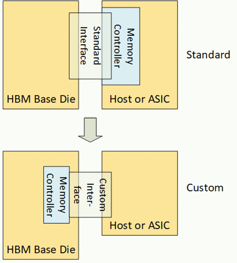
Fig. 1: In custom HBM, the memory controller no longer needs to drive between chips, so it can be much smaller, providing beachfront benefits. Source: Bryon Moyer/Semiconductor Engineering
The base die needs a logic process more advanced than a traditional DRAM process, but it doesn’t need to be as expensive as the host process. So the controller adds space to the base die while saving space on the host die. But the area it adds on the base die costs less than the area it saves, making it a net cost win.
Another cost saving occurs if the custom interface requires fewer connections than the standard one. The memory PHY area includes all the pads and drivers for external signaling. The controller no longer connects to the host and HBM stack because it’s buried in the base die, but it may still need all the original signals. Yet because they don’t talk to another chip, they don’t require pad space, so they can have less advanced drivers.
“You have the memory controller sitting on the logic compute die,” Malik explained. “You put the memory controller onto the custom HBM base die and remove the PHY [since it no longer drives between chips] because the PHY is the biggest block sitting on the compute die, and that PHY is just for connectivity. So remove the PHY and put on UCIe or another die-to-die interface. That is around 70% smaller than a standard DRAM PHY. It enables 25% more compute capabilities on the compute die. It reduces the overall power, and it increases the efficiency of the whole XPU die.”
A key benefit comes from the ability to connect to more HBM stacks. “It depends upon the die size of the XPU, but now you have more shoreline, so you can connect more HBMs to provide more memory capacity for those compute tiles,” said Malik.
The memory-maker’s role in this effort is to provide a “TSV PHY,” which is IP that acts as a TSV template for the base die. Consider HBM5, for instance. “You’d have 2,048 bits connecting to this thing called the TSV5,” said Kruger. “That’s IP from the memory maker that connects to their stack of dies, and also directs how to interface with those connections and do tests.”
Of course, customization can go beyond just the interface. Companies may also want to tweak other features. “There are standards for RAS [reliability, availability, serviceability], but then people have their own thoughts on what’s needed and how they want to do that as well. So that’s an area where things get customized,” said Kruger. “You’ll have a control and management unit that will have this RAS telemetry aggregation and collection. How you send it to the rest of the system needs to be defined to understand how it fits in the larger system.”
Who designs these things?
While customization could be limited to the controller move, that’s unlikely, because it’s simpler to make other beneficial changes when the device is open. But there’s no set way to do this, and each project is likely a negotiation.
The four basic steps to consider are design, manufacturing (and wafer test), assembly, and final test. Of the four, design is the hardest piece because the others become more a matter of capacity. Design requires a team, tools, and a vision of how more memory can impact performance and power. In the past, that might have limited the companies capable of doing this to the memory makers or fabless companies, but today the hyperscalers have deep expertise in semiconductor design.
In that order, the first option seems unlikely. Memory makers are plenty busy with what’s on their plates, and taking on custom design may not fit well. We can’t speak for all the memory folks (and most didn’t want to talk on the record), but at least one company is concerned about being expected to do custom base die designs.
“Now, everything the customer wants is custom because they want higher bandwidth, ” said Jaesek Lee, vice president of package engineering at SK hynix America, in a presentation. “But memory companies need to do the design and manufacturing [of custom HBM], and we are resource-constrained.”
Synopsys’s Kruger seconded the resource issue, noting that it’s a big lift to do one of these projects. “These people don’t have teams waiting around to do all these custom designs,” he said. “You need to have a significant volume to justify a custom development like this, so it’s going to limit the number just based on that.”
If the memory guys are out, that leaves fabless folks and the hyperscalers. It’s not clear how many fabless companies will be involved in this, but given Marvell’s project, it’s reasonable to expect others will do this, as well.
Still, each such project is custom. “It is really essential to work with the end hyperscaler customers,” said Malik. “Even though you can stitch blocks together, tuning and optimizations are still required. And every hyperscaler is different.”
Who builds the stack?
For standard HBM4, the memory maker gets the tested logic die from the logic foundry, assembles the stack, tests the finished product, and ships it. For a custom version, the memory maker still builds the memory dies for the stack, but it no longer owns the base-die design. Do they still take the custom base die and build the stack? Do they have the capacity to do that in a market like the one we have now?
It turns out there’s no single answer on who will perform stack integration. Each project will spin up by forming an agreement between a memory house, a logic foundry, and perhaps an assembly facility that can handle stack bonding (expected to be hybrid bonding for HBM4E and after, at least for 16-high stacks). Who owns that flow can vary by project.
“There are different business engagement models with different customers,” said Malik. “Some customers give full ownership of the logic to the guys designing it while taking full ownership of the integration. Some give the logic guys certain responsibilities and memory guys other responsibilities. And in some cases, there are customers who like to take full ownership themselves by working with a logic partner as well as with memory partners.”
In recent news, TSMC announced it was working with Winbond. Winbond will provide memory wafers while TSMC assembles the stack. The headline there was that this took pressure off the other three main memory makers.
A poor-person’s HBM?
Given memory shortages, designers have to be more creative about how to get enough memory — especially for companies that may not be near the top of the list of who gets memory allocation. An alternative stacks standard DRAM dies atop a host.
These assemblies aren’t as tall as a true HBM stack, but they may integrate as many as four DRAM dies atop one another. Even though HBM hasn’t moved to hybrid bonding yet, other DRAM dies have.
“In designs that have already taped out, the bottom logic die is flipped face up and hybrid bonds connect to the downward-facing DRAM wafer on top,” explained Kruger. “That DRAM wafer has a <10‑µm bond pitch, so while HBM is still on microbumps, DRAM on logic is already on hybrid bonds.”
Whether stacking regular DRAM or HBM layers, the pitch is critical to the bonding technology. “Stacking memory requires robust TSVs, reliable bumps, bonding or interconnects, and strong materials for HBMs to continue scaling,” said Prahalad Parthangal, technical director for advanced packaging at Lam Research in a presentation at the SEMI Strategic Materials Conference. “When the pitch scales below 10µm, the hybrid bond interconnect becomes a key enabler.”
One might think this approach is a response to tight memory supply, but it turns out there is an even more important reason — speed.
“We thought that that was [happening] because some customers can’t get HBM,” said Kruger. “An application-level reason is that it gets you significantly lower latency because now you’re using hybrid bonds or bumps that are tightly spaced to do the transfer — and lower power as well.”
Synopsys expects fewer than 20 projects per year to be implemented this way.
It all varies per project
Rounding all of this up, here’s how each of the major four steps happens:
- Design will vary by project, but it most likely will be performed either by the company consuming the custom memory (such as a hyperscaler) or by a design house, particularly one that offers customization.
- Manufacturing and wafer test will happen at a logic foundry, although it may or may not be the same foundry that makes the standard base die.
- Assembly will vary by project. The owner will be determined as part of the project agreement.
- Final test can proceed as it did with standard HBM, but with a custom test program.
With projects underway now, custom HBM stacks should be hitting datacenters in a year, or maybe two.
And how might this impact memory supply? It may feel like custom HBM comes in addition to normal HBM supply requirements, but when you add up what the industry will require for memory, that demand doesn’t specify whether the memories are standard or custom. So this isn’t expected to further burden capacity. Instead, it’s a question of mix.
It may still be difficult to acquire a supply, however. “There is a huge shortage for memory, and prices are skyrocketing,” cautioned Malik. “These memory suppliers have sold out their fabs for the next year and a half or two years.”
How that mix settles out could challenge supply planning, since it’s easy to plan for the standard implementations. Predicting who will do custom versions, and where that manufacturing will take place, could make those forecasts a bit wobblier.
—Ed Sperling contributed to this report.
Related Articles
HBM4 Sticks With Microbumps, Postponing Hybrid Bonding
Process cost and yield issues delay the adoption of hybrid bonding.
Flash Getting Stacked High-Bandwidth Version
Inspired by HBM, HBF could improve AI efficiency in 3D flash memory.
How To Build Billions Of Bumps
Hybrid bonding permits unprecedented connection density.
The post How Will The Custom HBM Business Work? appeared first on Semiconductor Engineering.