微信内可能无法直接打开本站。请点右上角 ··· → 在浏览器打开,或复制链接。
CFETs Forge Better Connections
RSS 官方收录 · 可信分层展示
关键摘要
Key Takeaways: Intel, Samsung, TSMC, and IBM are choosing different ways to connect nanosheet tiers, but all will use direct backside vias for backside power delivery.…
- At the heart of CFETs are defect-free epitaxy, ALD dielectrics, workfu…
- Virtual simulation speeds pathfinding, integration, and yield-improvem…
- In just a handful of years, the leading-edge device makers will begin …
摘要引擎:抽取
正文提要
Key Takeaways:
- Intel, Samsung, TSMC, and IBM are choosing different ways to connect nanosheet tiers, but all will use direct backside vias for backside power delivery.
- At the heart of CFETs are defect-free epitaxy, ALD dielectrics, workfunction-optimized metals, and perhaps layer transfer.
- Virtual simulation speeds pathfinding, integration, and yield-improvement efforts while saving the time and cost of actual silicon development.
In just a handful of years, the leading-edge device makers will begin rolling out CFETs (complementary field effect transistors), nearly doubling the transistor density of today’s lateral nanosheets by taking those p- and n-type transistors and stacking them one on top of another. The new architecture is expected to improve packing density by 40%, deliver a 50% performance leap, and potentially provide a 70% efficiency gain. [1]
Optimizing the materials and process flows for CFET gate-stack fabrication is a major feat. The next big challenges will be making all the necessary vertical connections between the various signal and power lines to, from, and between transistors, as well as the wafer backside.
While process qualification is years off, early research shows TSMC, Intel, Samsung and IBM taking slightly different approaches to CFET construction. For example, IBM slightly offsets the first set of transistors, which are fully fabricated before the second set in a sequential flow.
Most others are pursuing monolithic process flows, where the entire stack is built at the same time. Intel is exploring monolithic flows, as well as a hybrid-substrate approach that uses the best silicon substrate for each transistor, boosting the pFET that historically performs worse than the nFET. TSMC is using a backside gate contact and two versions of vertical contact plugs to connect different functional layers in SRAM bit cells. And Samsung has developed a novel dielectric stack to separate the two gate regions.
Alongside each of these efforts, multi-physics simulation plays an increasing role in pathfinding and yield optimization for these new structures. Potential problem abound. Even a few nanometers of out-of-place material can cause catastrophic yield loss. And warpage on the micro- or nanoscale can significantly impede device performance.
“When you talk about nanosheets, they are just so small. There’s almost no room for variation,” said Joseph Ervin, managing director of Semiverse Solutions at Lam Research. “When things deform, that potentially causes a problem, and that’s what we see. Even a two-nanometer misalignment can cause a big problem for manufacturing.”
Others agree. “You have to balance every innovation with warpage and reliability,” said Lalitha Immaneni, vice president at Intel assembly test technology development. “That’s the approach the EDA ecosystem is taking in writing all these multi-physics modeling tools. We need to get better at predictability. If you have thousands of designs, you can create a bank, and then at every milestone in the design — whether the design is 90% complete or 60% complete — you should be able to create it, complete it, and say, ‘Hey, here are the four or five options for how I want to disperse the copper density. These are the two best options.’ But if you tell me a week before tape-out that a complex product might warp, or copper density variation is too high, it’s too late.”
Backside power delivery, first introduced at the 2nm node, adds more complexity and a greater opportunity for warpage, variability, and defectivity. “As demonstrated by companies such as TSMC and Intel, these approaches require advanced wafer bonding, backside thinning, and highly accurate frontside-to-backside alignment processes,” said Douglas Guerrero, senior technologist at Brewer Science. “These new integration requirements add significant manufacturing complexity while increasing sensitivity to process variation.”
Although new transistor architectures are first implemented in advanced logic, the technology trickles down to other platforms. “The first 3D effect was achieved with finFET technology, and now with the introduction of the gate-all-around technology we are continuously advancing innovation toward full 3D transistors,” said Jaihyuk Song, corporate president and CTO at Samsung in a recent presentation. “Logic devices at Samsung were the first devices to adopt these technologies, and the same approach was extended to DRAM devices, followed by NAND. By rolling out these innovations across the three basic devices, we not only achieved the primary performance gains but also created library packs that create synergy throughout the entire company.”
At first, it seems that stacking one transistor on top of another would reduce the lateral width by 50%, but it’s less than that to make room for connections between the top and bottom transistors, and from the FETs to signal lines above and the power lines below. Nonetheless, CFETs will likely reduce standard-cell height from ̴5T (5x contacted pitch) to 4T or less, depending on the process. The increased density becomes especially compelling in SRAM designs where it can enable a move from a 6T to a compact 4F2 construction.
Nanosheet transistor flow and priorities
To form nanometer-level silicon sheets through which current flows (channels), an epitaxial process first grows a silicon/SiGe heterostack with a number of layers corresponding to the number of nanosheets. For instance, a minimum of 6 silicon layers and 5 SiGe layers are needed to form a 3-nanosheet nFET over a 3-nanosheet pFET, or vice versa. The SiGe is sacrificial, so it is selectively removed (a.k.a. channel release) to leave suspended silicon bridges, while the regions at the ends form the source and drain.
Chipmakers ramp up drive current by adding more sheets, but this significantly increases process complexity, making a 3-sheet transistor much harder to fabricate than a two-sheet one. Chipmakers tend to place the nFET sheets on top and the pFET sheets below so the latter benefit from the greater stress induced by the first Si/SiGe stack, increasing mobility.
CFET nanosheet channel width varies between ~11nm and 25nm, but it is only a few nanometers thick. The nanosheets are surrounded by a thin high-k gate dielectric and then fully surrounded by a metal gate, both deposited by atomic layer deposition (ALD). A major difference between GAA and CFET flows is the addition of a middle dielectric isolation (MDI) region, which isolates the top gate from the bottom gate.
For example, Samsung fabricated 42nm gate-pitch CFETs with triple-stack channels for both transistor types, where its MDI layered stack contains three different germanium concentrations. “To enable independent tuning of the gate dipole and work-function metal for n- and p-FETs, we introduce three epitaxial layers for the MDI between top- and bottom-tier gate regions,” noted Samsung’s Hwang Dong-hoo, principal scientist at Samsung Electronics’ R&D Center, in a recent presentation. [2] “The MDI structure for vertical gate patterning is a critical enabling technology for applying appropriate gate dipoles and metals for n- and p-FETs, respectively,” said Dong-hoo.
The MDI is formed after dummy gate formation in the flow, which includes the following steps:
- Wafer preparation
- STI formation
- Dummy gate formation
- Bottom S/D etch
- Bottom S/D growth
- S/D isolation formation
- Top S/D growth
- GAA formation
- Replacement metal gate
- MOL formation
- BEOL integration
TSMC, for its part, emphasizes the transformative nature of CFET technology and the options it offers. “In addition to the scaling benefits, this vertical stacking architecture also introduces new opportunities for flexible front- and back-side pin access. These advancements fundamentally reshape the design infrastructure, enabling enhanced interconnect routing and power delivery optimization strategies,” explained Szula Liao, director of R&D Pathfinding and Device Architecture Pioneering at TSMC. [3]
The process flow is given as:
- Nanosheet stack formation
- STI formation
- Dummy gate patterning
- N/P source/drain epitaxial integration
- ILD-0 planarization
- Nanosheet cut isolation
- Si nanosheet channel release
- Gate stack & multi-Vt integration
- MOL and BEOL integration
- Backside MOL and BEOL integration
As part of the gate stack, TSMC uses a dipole patterning process to deliver both higher and lower threshold-voltage tuning for GAA transistors and CFETs. Here, ultra-thin metal-oxide dipole layers (such as lanthanum or aluminum oxides) at the high-k gate dielectric interface shift the transistor work functions electrostatically without changing the gate metals. “Multi-Vt is a critical platform technology feature, allowing designers to optimize performance and energy efficiency by mixing transistors with different speed/power characteristics (e.g., high-Vt for low power, low-Vt for high speed) on the same chip. This capability is vital for complex AI and mobile device systems,” according to Liao. [3]
Because nFET and pFET transistors offer peak carrier mobility (and thus higher frequency) on different silicon substrates, chipmakers can use different substrates to fully optimize performance. Intel chose (100) silicon for the nFET (as is typical), but (110) crystalline silicon for the pFET, which it then precisely joined using a layer-transfer method. This process starts by temporarily bonding a device wafer onto a donor wafer, bonding the donor to the active target wafer, and then cleanly removing the donor wafer with perfect alignment.
The result is a 3X effective mobility gain using pFET on (110) stacked on nFET on (100). [4] In its 2×2 RibbonFETs at 45nm gate pitch with direct backside power via, the transistors share a common gate, so it employs transistor depopulation to avoid the complexity associated with a split-gate approach. Design-technology co-optimization features compensate for associated performance reduction.
For its CFET designs (which it licenses to Rapidus), IBM is pursuing a sequential approach with slightly staggered transistors. Staggering allows more direct connections of signals and power lines to the transistors than a direct vertical stack. By shifting the top nanosheets by 10nm, the company stated that it saved 20nm in cell height. The company also emphasized that the design could be patterned with existing lithography capabilities, achieving bottom active-to-active spacing of 50nm, top active-to-active spacing of 30nm and gate cut thickness of 20nm, which, along with other connections, yield 40% cell height scaling compared to today’s non-stacked nanosheets. [5]
By comparing process windows across architectures, engineers can identify which design offers greater tolerance to manufacturing variations, fewer defects, and better overall performance. “The design engineer generally knows ‘this is exactly the device I want at the end of processing,’” said Ervin. “But how do I make that? That’s where the ingenuity and the art of making transistors comes in. Simulation is a good starting point because it uses physics-based models. Engineers are comparing putting nFET on top of pFET, or vice versa, and evaluating different integration schemes.”
Simulation also can be used to optimize a technology once it is finalized. “Where we see a lot of interest now is in taking the initial nominal process case and injecting variation across it for each of the process steps to see what the outcome is going to be,” said Ervin. “We use machine learning to map the entire space around the nominal case, which provides a process window for each process step and the variation around it. You have an idea generally of what the equipment capabilities are, like a deposition thickness or an epitaxial control etch depth and selectivity between materials, which you feed into the model right away.”
Importantly, IBM also demonstrated high-NA EUV patterning of 21nm metal lines using single exposure, replacing the more complex first-gen NA EUV with self-aligned litho-etch litho-etch multi-patterning, achieving even better electrical results.
CFETs require atomic-level control
The main fabrication challenges for today’s nanosheet (gate-all-around, GAA) transistors extend well beyond just making the nanosheets. They also entail maintaining extremely tight control over critical dimensions, spacing, release (SiGe removal), gate formation, and contacts across the 300mm wafer.
In addition, although many gate-all-around transistors employ backside power delivery, all CFET flows will, according to imec’s roadmap (see Figure 1). Interestingly, although many experts talk about an end to feature-size scaling, the roadmap indicates continued shrinking of metal pitch using higher-NA EUV lithography, though scaling is modest compared to historical levels.
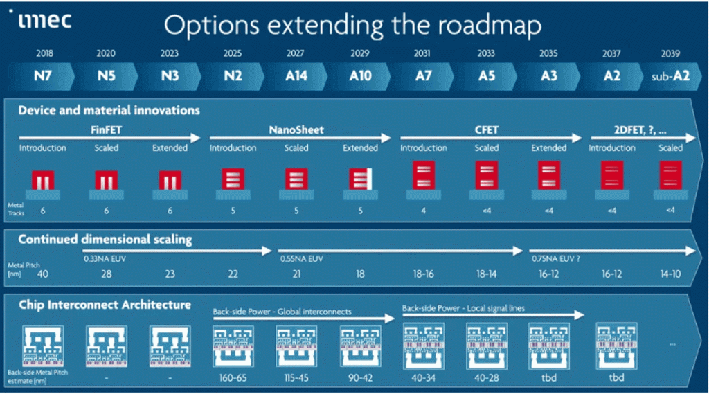
Fig.1: The roadmap shows first CFET production at the A7 node around 2031 with critical dimension scaling below 18nm. Source: imec
EUV patterning faces two problems as a direct result of the low total photon count per unit area (i.e., shot noise), which leads to variation in photon absorption, line-edge/width roughness (LER/LWR), and stochastic defects. At the same time, features are often taller to achieve higher aspect ratio etching, so pattern collapse is a concern.
EUV underlayers can help. “EUV underlayers play an important role in improving lithographic performance by enhancing resist adhesion, reducing pattern collapse, and improving overall pattern fidelity,” said Brewer Science’s Guerrero. “Advanced underlayer materials can also help reduce line-edge and line-width roughness and, in some cases, lower required exposure dose by improving the chemical environment of the resist and mitigating stochastic defects.”
Another technology that can address LER and LWR by etching away the rough edges is ion beam etching. IBE accelerates a highly collimated beam of ions at the resist pattern, and the beam tilt angle must be optimized for the process.
EUV patterning and etching involve multi-layer optimization. “Silicon-containing hardmasks are commonly used during pattern transfer. After EUV exposure and development, the resist pattern is transferred into the silicon hardmask and subsequently into an underlying carbon layer,” Guerrero said. “Because the resist, silicon hardmask, and carbon layer exhibit different etch selectivity, the pattern transfer process can be precisely controlled through the choice of etch chemistries. This approach improves critical dimension control, pattern fidelity, and process integration flexibility.”
Virtual fabrication’s role
Even before silicon starts, companies turn to virtualization to compare the many integration options. “The real challenge I’ve seen is people can think in planar technology actually quite well. Once you switch into the third dimension, it becomes much more difficult to keep track of what’s happening,” Ervin said. “With CFETs, now you’re adding another stack on top of a completely different stack, and it’s very complex. So that’s where you need computers, because you’re trying to achieve atomistic-level accuracy. Any variation can have huge implications on yield.”
Virtual fabrication and digital twins of processes dramatically reduce the number of actual wafers that need to be run in process development. “One important application of AI and machine learning is the creation of digital twins that simulate fab operations and process flows, reducing the need for costly and time-consuming physical experimentation,” said Guerrero.
By comparing process windows across architectures, engineers can identify which design offers greater tolerance to manufacturing variations, fewer defects, and better overall performance. “The design engineer generally knows, ‘This is exactly the device I want at the end of processing,’” said Ervin. “But how do I make that? That’s where the ingenuity and the art of making transistors comes in.”
Simulation also can be used to optimize a technology once it is finalized. “Where we see a lot of interest now is in taking the initial nominal process case and injecting variation across it for each of the process steps to see what the outcome is going to be,” said Ervin. “We use machine learning to map the entire space around the nominal case, which provides a process window for each process step and the variation around it. You have an idea generally of what the equipment capabilities are in terms of deposition thickness or an epitaxial control etch depth and selectivity between materials, which you feed into the model right away.”
Language models may be employed, as well. “AI gives you another engine to explore this space,” said Erivin. “We can use it to say, ‘I want to have no failures of these types in my technology. Can you find me something in the process integration flow to target those and make it manufacturable?’ The AI component can answer some of these questions. That really makes this an exciting field.”
Conclusion
The CFET architecture is an exciting development for the semiconductor industry, increasing device density dramatically while promising 50% performance improvement and 70% less energy consumption. The early CFET publications out of TSMC, Samsung, Intel, and IBM are proving that although they all use the same basic processing tools of epitaxy, ALD, and etching, the process flows are slightly different. Companies are deciding between so-called split-gate processes with dielectric isolation and shared-gate with a depopulation approach that reduces parasitic effects.
Although we think existing nanosheet transistors (i.e., non-stacked) are nearing the point where variation, warpage, and alignment issues are becoming untenable, CFET generation will need to do even better. By the time of production roll-out, around 2031, high-NA lithography will be more mature and simplify flows. Virtual fabrication is likely to play an even more pronounced role in pathfinding and yield improvement than it does today.
References
- Samuel K. Moore, “Future Transistor Stacking Plans Start to Diverge, IBM chooses a different path from Intel, Samsung, and TSMC,” IEEE Spectrum, June 25, 2026,
- S. Liao et al., “CFET Demonstration for Future Logic and SRAM Technology,” 2026 IEEE/JSAP Symposium on VLSI Technology and Circuits (VLSI Technology and Circuits), Honolulu, HI, USA, 2026, pp. 1-3, doi: 10.1109/VLSITechnologyandCir65830.2026.11577430.
- J. A. Wiedemer et al., “Demonstration of CFET Inverters on Si (110) with 2X2 RibbonFETs at 45nm Gate Pitch with PowerVia and Direct Backside Contacts,” 2026 IEEE/JSAP Symposium on VLSI Technology and Circuits (VLSI Technology and Circuits), Honolulu, HI, USA, 2026, pp. 1-3, doi: 10.1109/VLSITechnologyandCir65830.2026.11577296.
- D. Hwang et al., “First Demonstration of 3D Stacked Fets at Gate Pitch of 42 nm Featuring Triple Stacked Nanosheet Channels for Advanced Logic Applications,” 2026 IEEE/JSAP Symposium on VLSI Technology and Circuits (VLSI Technology and Circuits), Honolulu, HI, USA, 2026, pp. 1-3, doi: 10.1109/VLSITechnologyandCir65830.2026.11577279.
- C. Zhang et al., “Area and Performance of Staggered-Channel Nanostack SRAM Bitcells,” 2026 IEEE/JSAP Symposium on VLSI Technology and Circuits (VLSI Technology and Circuits), Honolulu, HI, USA, 2026, pp. 1-3, doi: 10.1109/VLSITechnologyandCir65830.2026.11577402.
Related Articles
The Sub-2nm Paradox
Reducing variation in manufacturing, monitoring behavior over time, and targeting specific workloads can have a big impact on power, performance, and area/cost.
What’s Different About Next-Gen Transistors
Advanced etch holds key to nanosheet FETs; evolutionary path for future nodes.
Big Changes In Architectures, Transistors, Materials
Who’s doing what in next-gen chips, and when they expect to do it.
Backside Power Delivery Creates Fab Tool, Thermal Dissipation Barriers
Moving the power delivery network to the backside of a chip reduces congestion, but it introduces new challenges for fabs.
The post CFETs Forge Better Connections appeared first on Semiconductor Engineering.